At the 2018 Bay Area Maker Faire, our project Uncovering the Silicon showed off a number of simple and complex integrated circuits (with rather large feature size) under the microscope. We had a great time helping visitors look at the features and get a glimpse of what’s inside those black box integrated circuit packages. To take this to the next level for this year’s Maker Faire, we decided to try and close the loop; to take one simple integrated circuit and elucidate its workings well enough that visitors to our booth will be able to see every single component of the circuit, understand their function, and relate it to the macroscopic behavior of the chip. For this, we picked what turns out to be a rather obscure chip: the Fairchild μL914, which is a dual 2-input NOR gate. This chip belongs to the resistor–transistor logic (RTL) family.
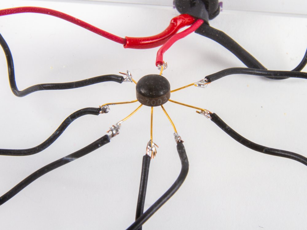
Here’s what the chip looks like. It’s in a funny old “glob-top” can package with eight leads.
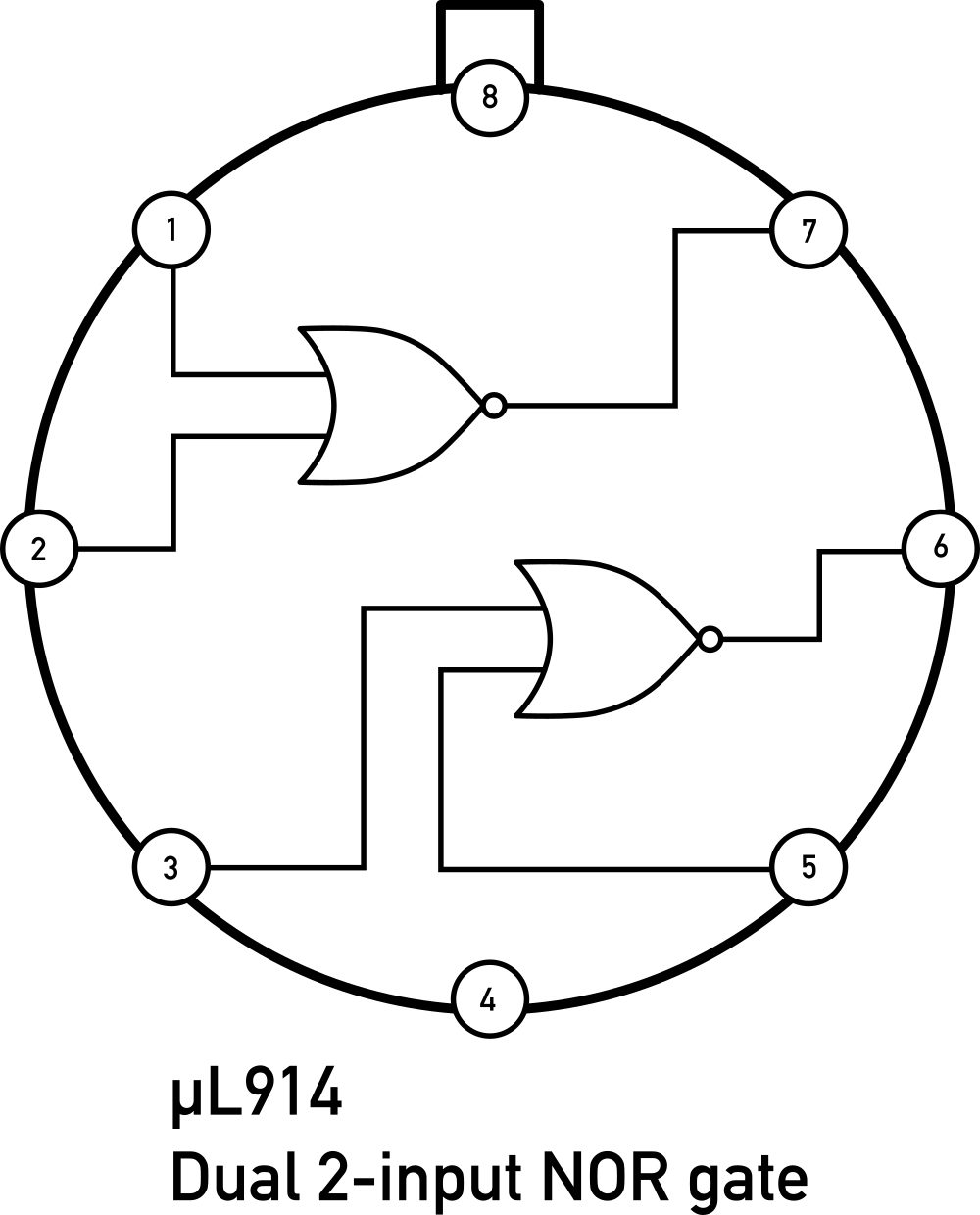
Here’s the pinout; there are two NOR gates in the chip, plus power and ground.
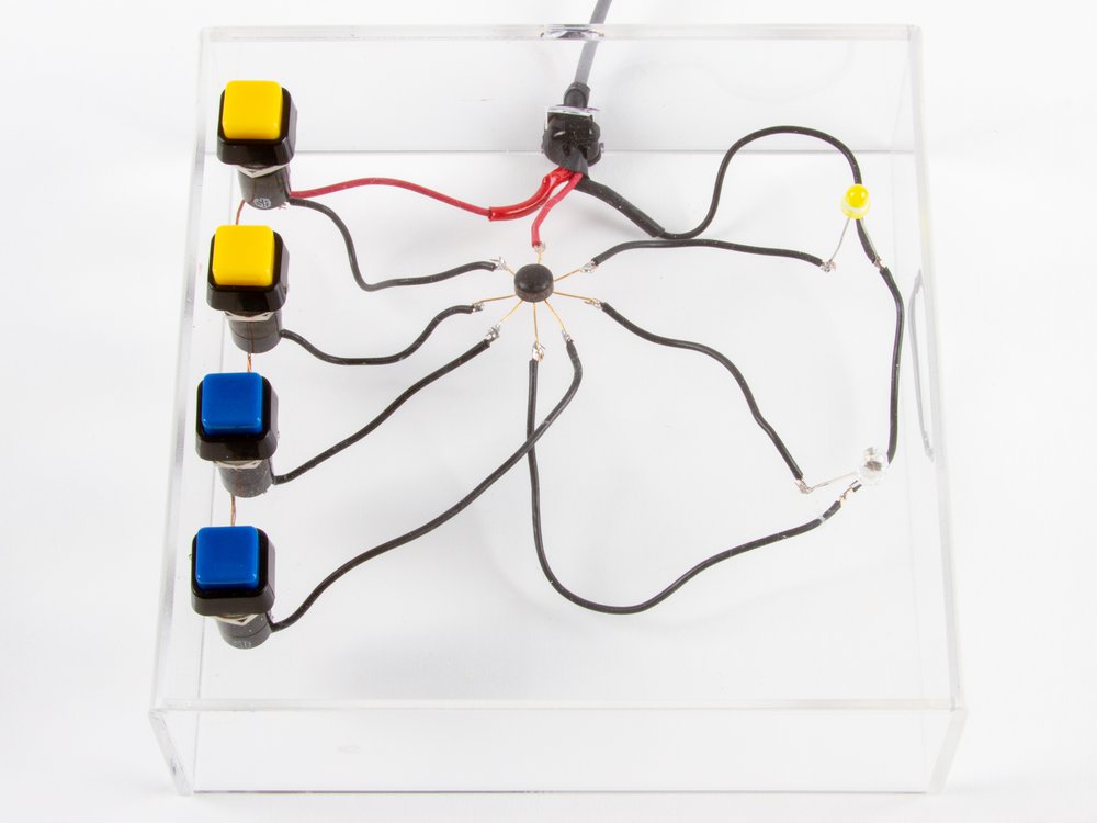
Ken Shirriff built a circuit with the chip to demonstrate its functionality. When we push either of the two buttons for one of the gates, that LED will turn off.

Here’s the schematic diagram, adapted from the original datasheet. If you look at the left side, if either of those inputs goes high, the transistor pulls the output low.
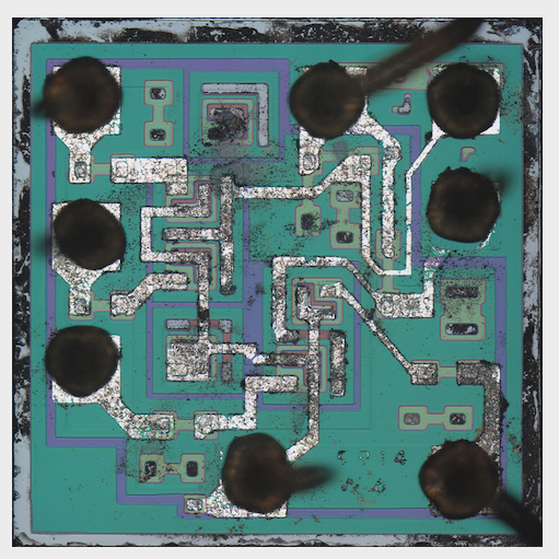
John McMaster decapped a few of the chips and sent us a die photo. He made a video about the process — no small feat. We’ll be bringing one of these bare chips and a microscope (equipped with both eyepieces and a camera) to Maker Faire.
For the macroscopic scale, we approached visualizing this circuit from a couple of angles: the physical structure of the chip, and the electronic structure of the circuit.
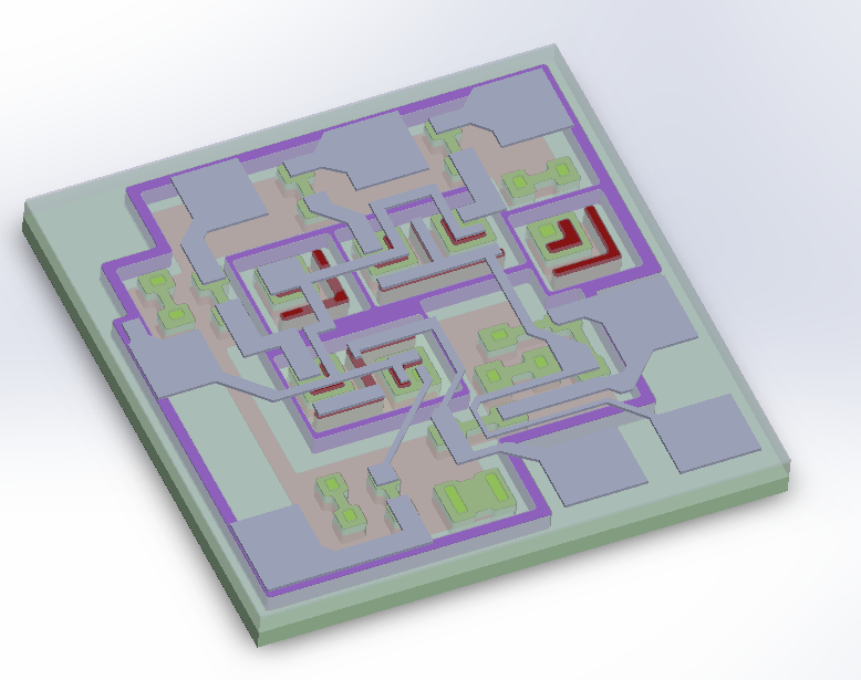
Eric Schlaepfer used the die photo to model the structure of the chip in CAD.
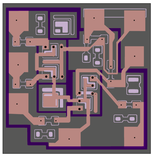
Simultaneously, Ken designed a printed circuit board version for use with discrete components that maintained the same structure as the IC.

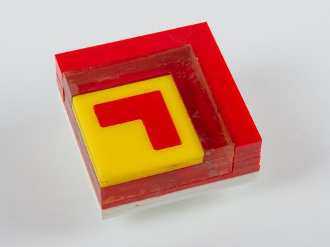
Working from Eric’s CAD model, we built a single NPN transistor model from layers of colored acrylic. If you lift it up, and look through the transparent middle layers, you can tell that the emitter (red) is embedded into the top of the base (yellow) and does not go all the down way through it. (Transistors like these are planar: The emitter is above the base, and the base is above the collector.)
The top layer of this little model has labels for the collector, emitter and base. It is removable so that the layers of the model can be more easily inspected.
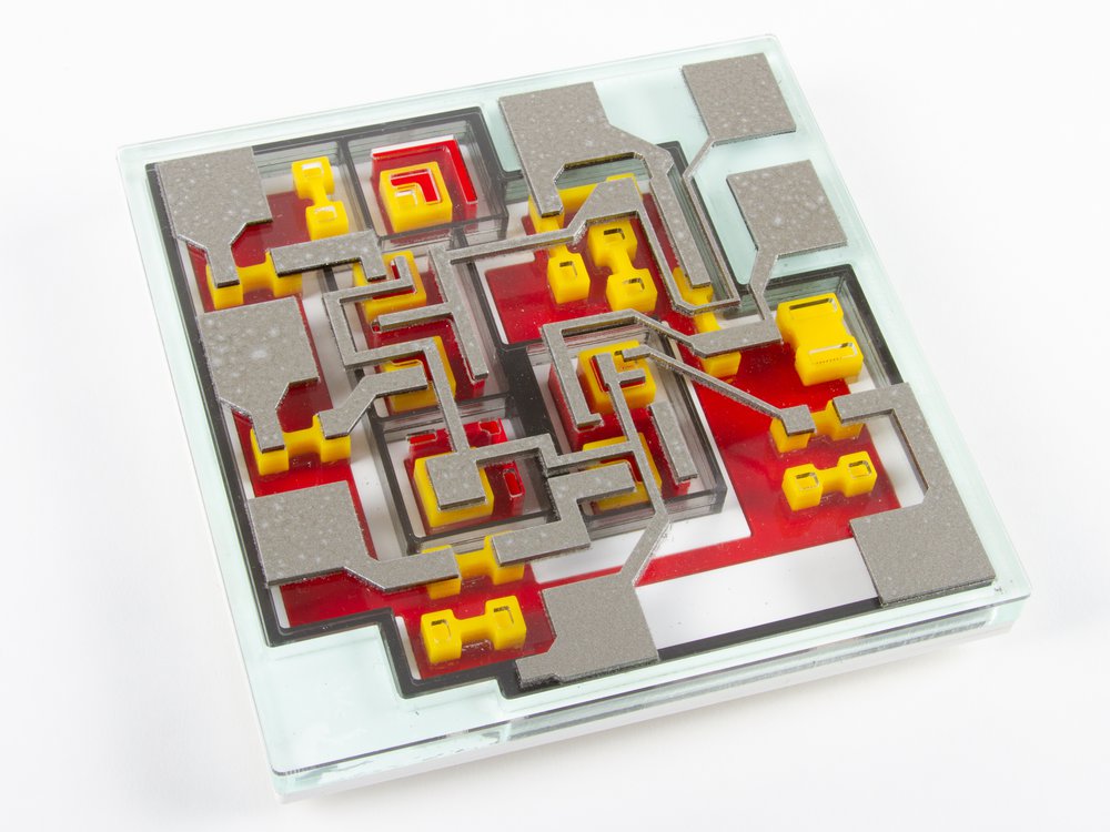
The model of the chip die includes a transparent cover representing the oxide layer, and that supports the metal layer with the wire bond pads on the edges.
One of the reasons that this particular chip is educational to look at is that there are a few unused components on the die. There are two unused transistors: one of them is unconnected, and the other is shorted. There are also several unused resistors (resistors are the dogbone shapes). The unconnected and unused components are easier to see, and provide a visual example that is useful for understanding what the connected components look like under the metal layer.
It is also fun to imagine what other circuits could have been made with different connections.
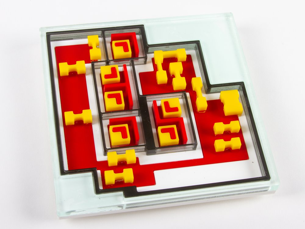
We glued most of the layers together, but left the top two layers removable so that it is easier to see the internal structure when the top is removed.
(Aside: we left out most of the epitaxial pocket material, because even though we used transparent acrylic to represent it, the layers of the components are much more visible without it present.)
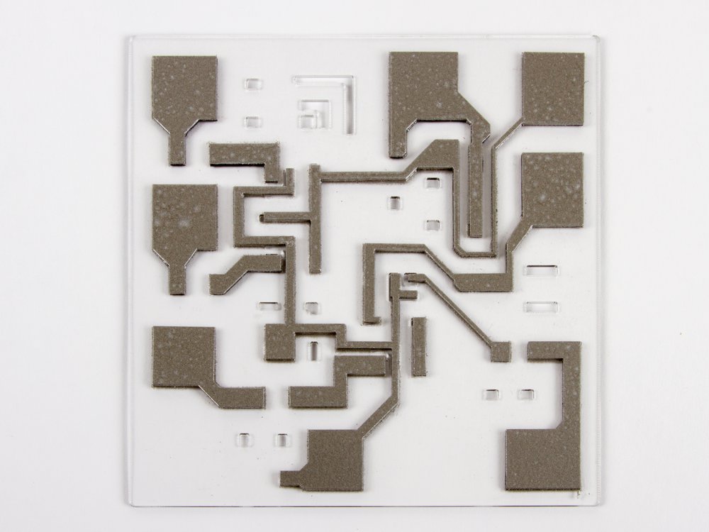
There are cutouts in the oxide layer where the metal layer connects to the circuitry below.
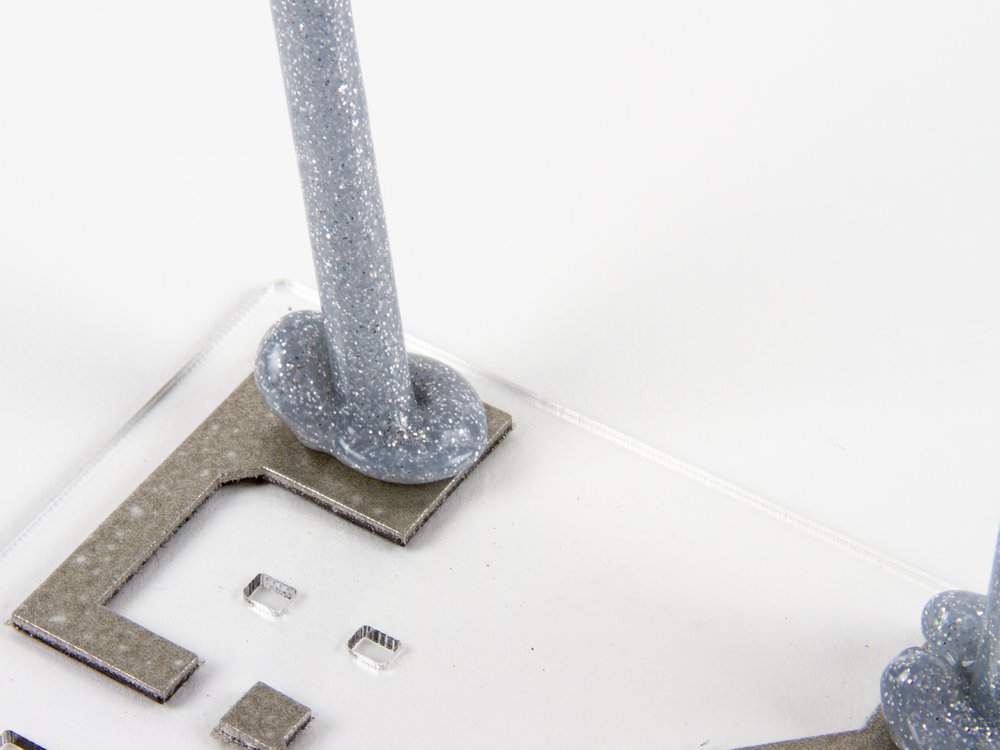
One of the most noticeable things you see when you look at this type of IC under the microscope is the bond wires. We’ve used silver glitter hot glue sticks to represent them.
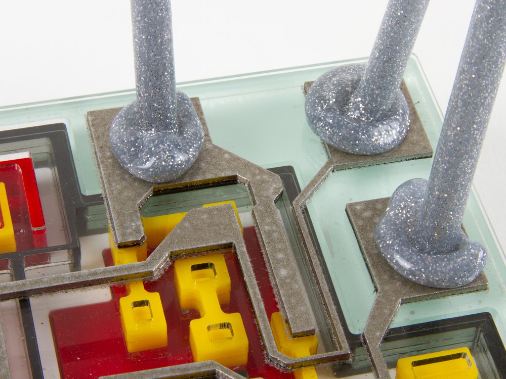
The glob of melted glue represents where the wire is bonded to the pad.
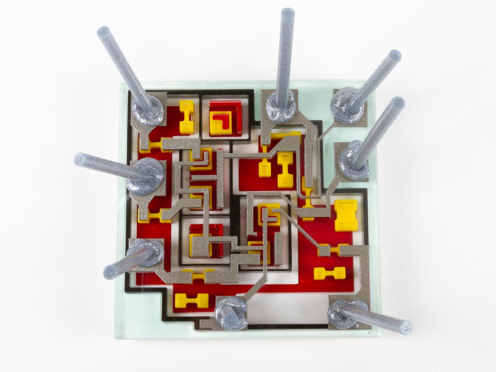
When you look straight down on the model with its glitter bond wires, it looks very similar to what you’ll see in the microscope.
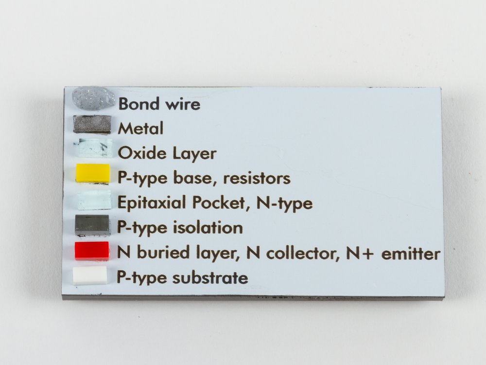
To round things out for our acrylic model, we made a physical legend to make it easier to identify all of the parts of the model.
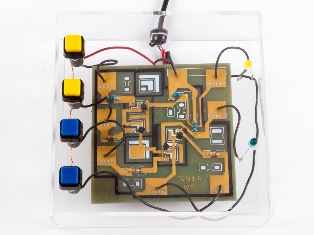
Once Ken got his PCBs back from our friends at OSHPark, he built it up with the same example circuit.
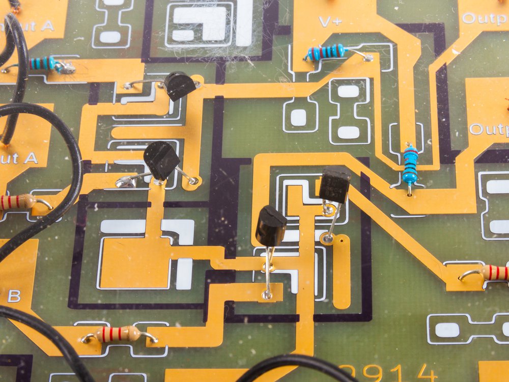
The PCBs turned out beautifully, and it’s great to see the familiar discrete packages on the enlarged circuit. Ken has published the PCB design on Github.
We hope to see you at Maker Faire this weekend!
Bonus: Ken laid out some hypothetical alternate metal layers to use the same die to create different chips.
Bonus video: Mike from Hackaday came to visit our project at Maker Faire and got a great video explanation of our project with Windell. He also wrote it up for Hackaday.


This is such a great idea for a Maker Faire project. Everything looks amazing – though the bond wires are an especially nice touch.
Have a good Faire!
I can see this being used as a differential amplifier. It could be turned into a long-tailed pair by tying the inputs of each NOR gate together to get two inverters and placing a resistor between the L914’s ground and the circuit ground. Another thought would be to use each input separately to get two inverting and two non-inverting inputs (I think it’s called a differential-difference amplifier). I’m not sure how well it would perform, though.
Great work!
I’d guess the 2 extra transistors were to make the 2-input OR gate version of the same part. (non-inverting)
That’s a good point! Some other possibilities might include a dual 3-input NOR, a dual NAND, or a hex inverter. There are probably others as well.
Excellent project!
One question, why the “L” shape in the transistor emitter?
Another question, the colors in the microscope image, do these come from interference? do they relate to film thickness?
So cool!
The different parts of transistors come in _many_ different shapes — some to increase boundary area, some for practical or space constraint reasons. (My favorite is the Scotty Dog.) In this particular case, it looks like they cut out the corner of the emitter to leave a place for the metallization to contact the base.
The colors appear to be formed by a combination of bulk properties and thin film interference.
This is such a cool project. I wish I had seen it last weekend – your booths have always been one of the highlights of MakerFaire and this time I had my 7-year-old daughter with me. This reminds me of your giant 555 and 741 chips that I still have displayed in my living room.
apparently if you pour LCD on the device it shows current flow
It would be interesting to de-cap a uL915 dual three input nor gate and see if the die was identical with a different metal layer. The die marking 9914 W6 is in the metal layer and it is the last layer so other parts could be made with the same base die. The uL915 that are on e-bay are in a TO77 metal can so it would be much easier to de-cap. The documentation on the uL915 on the web seems sparse but I have a 1985 ECG replacement catalog that does list some RTL circuits
I’ve seen lots of “extra” stuff on chips. Sometimes just the chip catalog number, e.g. 7404. When I was at Zilog, where we (not really me, I was officially in software) claimed to make the “Cadillacs” of processors, the die for the Z80000 32 bit CPU (at least at an early stage) had a silhouette of a car along one edge. I got to watch the silicon through a microscope while it was running diagnostics, although that didn’t make it look different!