Our reader Jon wrote in with a question about our open collector tutorial:
I really appreciated the tutorial, and I was able to follow along and understand it very well. One question I had was – what is the purpose of the 1 kilo-ohm resistor that is connected to the base of the PNP transistor? Because when the open collector is ‘high’ then the base of the transistor is at 12 V and it appears the 1 kohm resistor didn’t affect anything, and then when the open collector goes ‘low’ then the base is connected to ground through the output of the SN7407. So basically, what would the difference be if there was no 1 kilo-ohm resistor at all?
And, that’s actually an excellent question, about something that we usually gloss over.
The short answer is that this is a “base resistor” that we use to limit the maximum current that flows through the base of the PNP transistor. But, let’s take a look in a little more detail, and see what would happen if we didn’t have that there.
The High Case
First off, and as Jon does, let’s consider the case when the SN7407N input is high and its output is “high” (i.e., not pulled low). In that case, no current flows through the PNP transistor, and the 1k resistor does not affect anything. No current flows through that location, regardless of whether there is a resistor there.
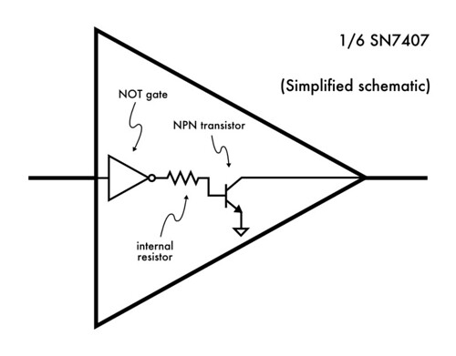
Let’s go over this case in more detail, starting with a reminder about what is in each of the six channels of that SN7407:
When a logical input to the SN7407N is high, the output of its internal NOT gate is low. Since the output of the NOT gate is connected (through a resistor) to the base of the internal NPN transistor, the base of the transistor is held low. Under these conditions the NPN transistor could be described as “off,” since it does not conduct current. And, as the output of the ‘7407 is connected directly to the (“open”) collector of the internal transistor, no current flows into or out of the SN7407N’s output.
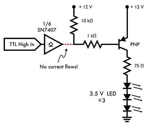
Because no current can flow into or out of the SN7407N’s output, to the rest of the circuit it is very much like the ‘7407 the chip is simply not there. Together, the 10 k? resistor (connected to +12 V) and the 1 k? resistor (which are in series) act as a single 11 k? “pull-up” resistor, and pull the base of the PNP transistor up to +12 V. Under these conditions the PNP transistor could be described as “off,” since it does not conduct current. Once equilibrium is reached (just microseconds after applying power), no current flows through the PNP transistor, no current flows through the LEDs, and no current flows through either the 10 k? or 1 k? resistor.
Since no current is flowing, the 1 k? resistor doesn’t actually make any difference; the circuit would behave exactly the same way if we only had the 10 k? resistor to pull up the base of the PNP transistor.
The Low Case
Now, let’s consider the opposite case, where the TTL input to the ‘7407 is low.
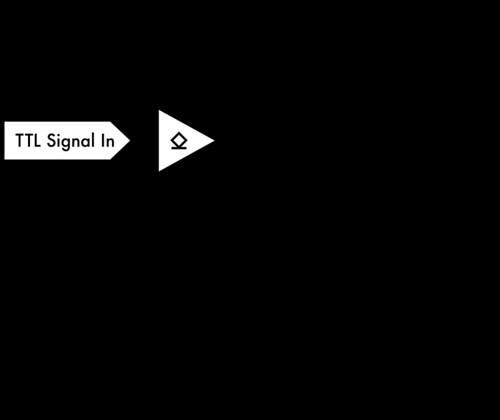
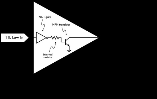
With the input low, the output of the internal NOT gate is high, which pulls high (and turns on) the internal NPN transistor, creating a low-impedance path from the output pin to ground. A small amount of current flows through the PNP transistor, through the 1 k? resistor, and through the NPN transistor to ground. That small current switches a larger current that can flow through the LEDs.
The two currents— small through the two transistors and larger through the LEDs —are illustrated above. Let’s try to estimate the amount of current that flows along each path.
On the higher-current path (through the LEDs), we have 12 V, the on-state emitter-collector voltage of the PNP transistor (roughly 0.3 V), the resistor (75 ?), and the three LEDs, each with forward voltage estimated at 3.5 V. The current through the LEDs is then roughly
I = V/R ? (12 V – (0.3 V + 3 × 3.5 V) ) / 75 ohms = 1.2 V / 75 ohms = 16 mA.
On the low-current path, we begin with 12 V, have the emitter-base voltage of the PNP transistor (a diode drop; about 0.7 V), the 1 k? resistor, and the collector-emitter voltage of the NPN transistor (maybe 0.3 V) to ground. The current flowing through these elements is then roughly
I = V/R ? (12 V – (0.7 V + 0.3 V) ) / 1000 ohms = 11 V / 1000 ohms = 11 mA.
As you can see, the current through these components is limited by the 1 k? “base” resistor, so called because it limits the amount of current that flows through the base of the transistor.
Aside: The “larger” current through the LEDs isn’t actually all that much larger. Why? Because our initial choice of 75 ? for the resistor was a bit too conservative. If the LEDs really do soak up a full 3.5 V each, then it might be better to use a somewhat smaller resistor to drive them.
And what if we didn’t have the 1 k? resistor?
The 1 k? “base” resistor limits the overall current through the PNP transistor and the NPN transistor inside the ‘7407 to a relatively safe 11 mA. Back to the original question: If we didn’t have that resistor there to limit the current, what would happen?
Electrically (and with some hand waving), the collector-base junction of the PNP and the base-emitter junction of the NPN each look like a forward-biased diode. So, we essentially have 12 V connected across those two “diodes” in series to ground, without any other elements. Without anything to limit the current, those two diodes are happy to allow a very large amount of current to pass, which can in some cased be limited only by the capacity of your power supply.
Naturally, this isn’t sustainable– one or both of them (the transistor and/or the chip) will fail, releasing their magic smoke. If your power supply isn’t well designed, it could also be the element (or one of the elements) that fails.
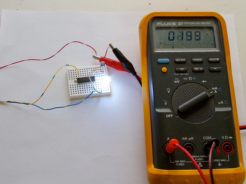
When we tried it (yes… yes, we did), we found that the current was limited to about 200 mA; only enough to “barely” destroy the SN7407 from overheating after a few minutes. Sadly (from the standpoint of taking exciting pictures) it did not puff up, blow its lid off, or anything quite so spectacular. It just stopped working.
With a fresh SN7407, and testing one part of the circuit at a time, we were further able to determine that the 200 mA limit is imposed by the SN7407 itself. How does it limit the current? Our best guess is that its own internal base resistors (in combination with finite transistor gain) serve to limit how much current can flow through its output transistor.
But then again, if you want your circuitry to work reliably, it’s better to not bump up against the limits of the hardware. The SN7407 has a recommended maximum output “sink” of 40 mA, and it lasted less than a minute when forcing it to sink a full 200 mA. And so the moral of our story: when using garden-variety transistors like these, don’t forget your base resistors.




This is such a good article! Great explanation and I really like the illustrations, especially the smoke. I don’t think I ever understood this so well until now. Thanks!
So what about if you bumped the 1k resistor upto 2k, 4k or even 10k? Wouldn’t that limit the current flow even more back through the SN7407, giving you a decent power savings, but also not affecting the actual working of the circuit?
Yes, to a certain extent. You can’t use an arbitrarily high resistor– giving you an arbitrarily small amount of emitter-base current through the PNP transistor –because the PNP transistor has finite gain. That gain is in the neighborhood of 100, if we used (for example) a 2N3906 transistor. If we want 25 mA collector current (i.e., the current through the LEDs) and have a gain of 100, then the “base current” (from the emitter to the base) needs to be at least 25 mA/100, or 0.25 mA.
We started with an estimated current of 11 V / 1000 ohms = 11 mA. With 2k, we’d have 5.5 mA, and with 4k, we’d have 2.75 mA. And with 10k, we’d have 1.1 mA. So, all of those should be fine and (as you note) give you a decent power savings without other consequence. But if you went as high as 50k, the base current would be 11 V / 50k ohms = 0.22 mA, and the transistor would no longer be able to switch as much current through the LEDs. And for higher yet values, the current through the LEDs would reduce rapidly.
Thanks for the info, that makes perfect sense. I’ve always wondered about how some of these values are figured out. And in some cases it seems to be really key, in others… not so much. Still black magic at times.
Fun to learn.
hi,
thanks for the explanation.
from your statements, as the base resistance increases, emitter to collector as well as emitter to base current flow decreases and vice versa. and when reaches a particular resistance the transistor stops switching. Am i right?.
It’s not so much that it “stops switching” as that it begins to allow an arbitrarily small amount of current to pass.
One small quibble that doesn’t negate any of the main points in the article:
When the base voltage of a BJT is equal to the emitter voltage (Vbe=0v), a small amount of leakage current still flows through the reverse-biased collector-base diode. That current produces a slight transistor action, allowing a small amount of current to flow from collector to emitter. To minimize the OFF-current, you need to take the base voltage slightly past the emitter voltage.. 0.1v-0.2v for most BJTs.
The leakage current is less than a milliamp, so for an entry-level tutorial, rounding it down to zero makes perfect sense. It is a detail of BJTs worth knowing eventually though.
Source: Motorola High-Speed Switching Transistor Handbook, http://archive.org/details/High-speedSwitchingHandbook — an amazingly complete reference on how BJTs are made, how they work, and how to design circuits that use them.
Thanks, Mike!