Our Sconic Sections post was highlighted in an article in the science section of today’s New York Times. The article covered several science and engineering topics in addition to geometric food (including George Hart’s Möbius bagel).
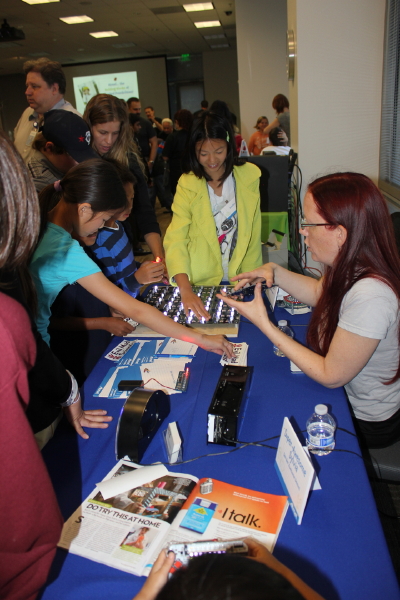
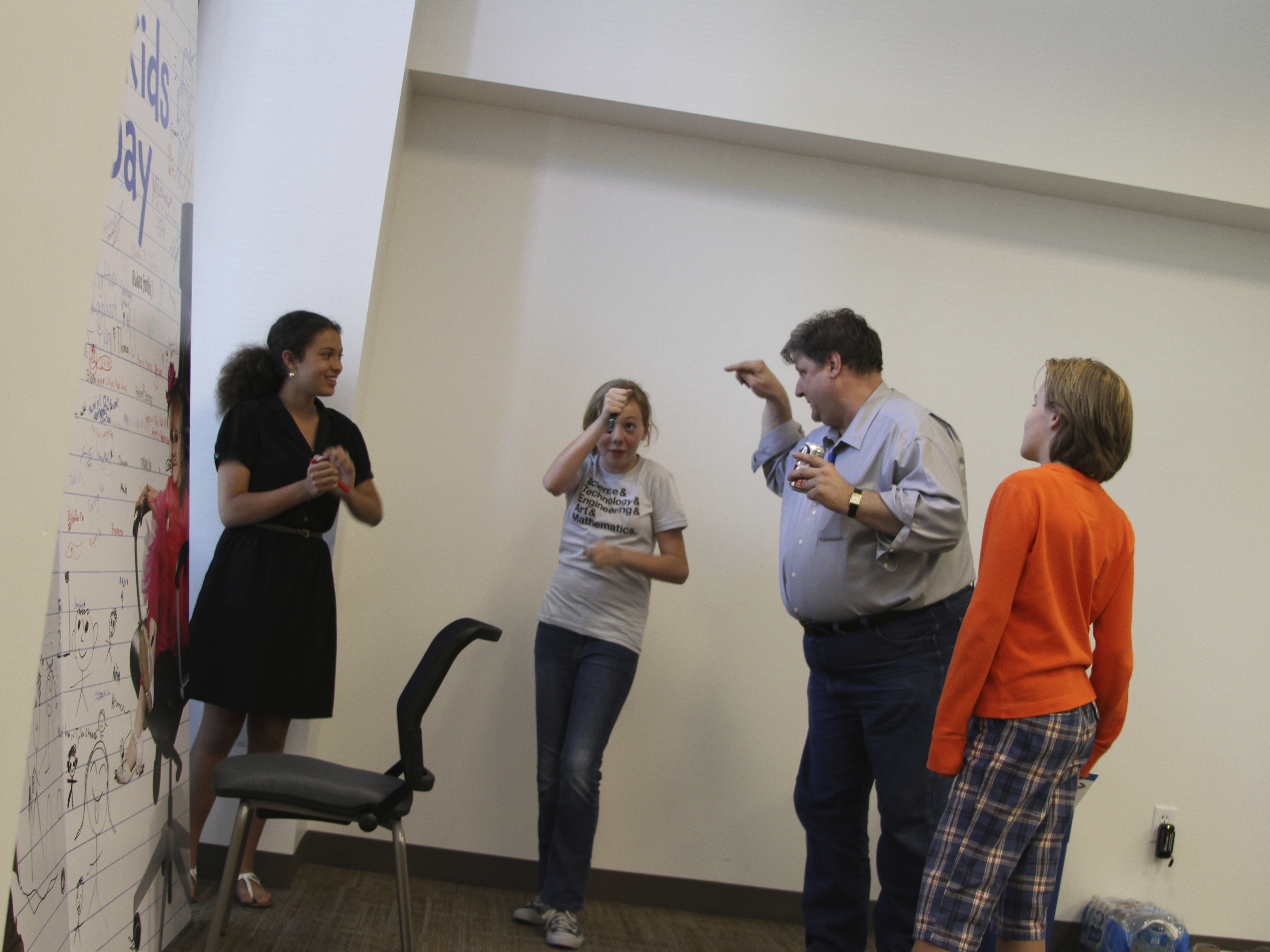
Super Awesome Sylvia and I were invited to attend Bring Your Kids to Work Day at Atmel recently. (Atmel, of course, is the company that makes the microcontrollers found inside Arduino products and in many of our own projects and kits.) We were there to help provide tangible, interesting, and playful examples of how Atmel chips can be used. And of course, we weren’t going to miss an opportunity to visit Atmel headquarters!
Photo courtesy of Atmel
The biggest hit with the kids were the Octolively interactive LED modules (sporting the Atmel ATmega164P). When the kids waved their hands over them, the LEDs would light up and ripple. Some of the kids would start out by poking and grabbing at the LEDs until they lit up, but as soon as I told them it would work “even without touching it” their eyes would get big, and they’d wave their hands over the top, enthralled.
Some of the other things we brought were our handheld game, the Meggy Jr RGB (with the ATmega328P); a Bulbdial Clock (Atmega328P again), which points rings of LEDs at different heights down at a central point to create shadow hands of different lengths; our giant Alpha Clock Five (ATMega644A); and the Larson Scanner (ATtiny2313A), which lights up nine red LEDs to make a scanning robot eye.
Photo courtesy of Atmel
Another project that captured the kids’ attention was a Keepon by BeatBots. Other demonstrations included a quadcopter and a hacked hexabot.
Photo courtesy of Atmel
We got to have lunch in the bright sun in the courtyard with Avary Kent, who was demonstrating the PuzzleBox, a brain-controlled helicopter.
Photo courtesy of Atmel
Sylvia got to give the PuzzleBox a try, triggering it to fly as soon as she concentrated hard enough.
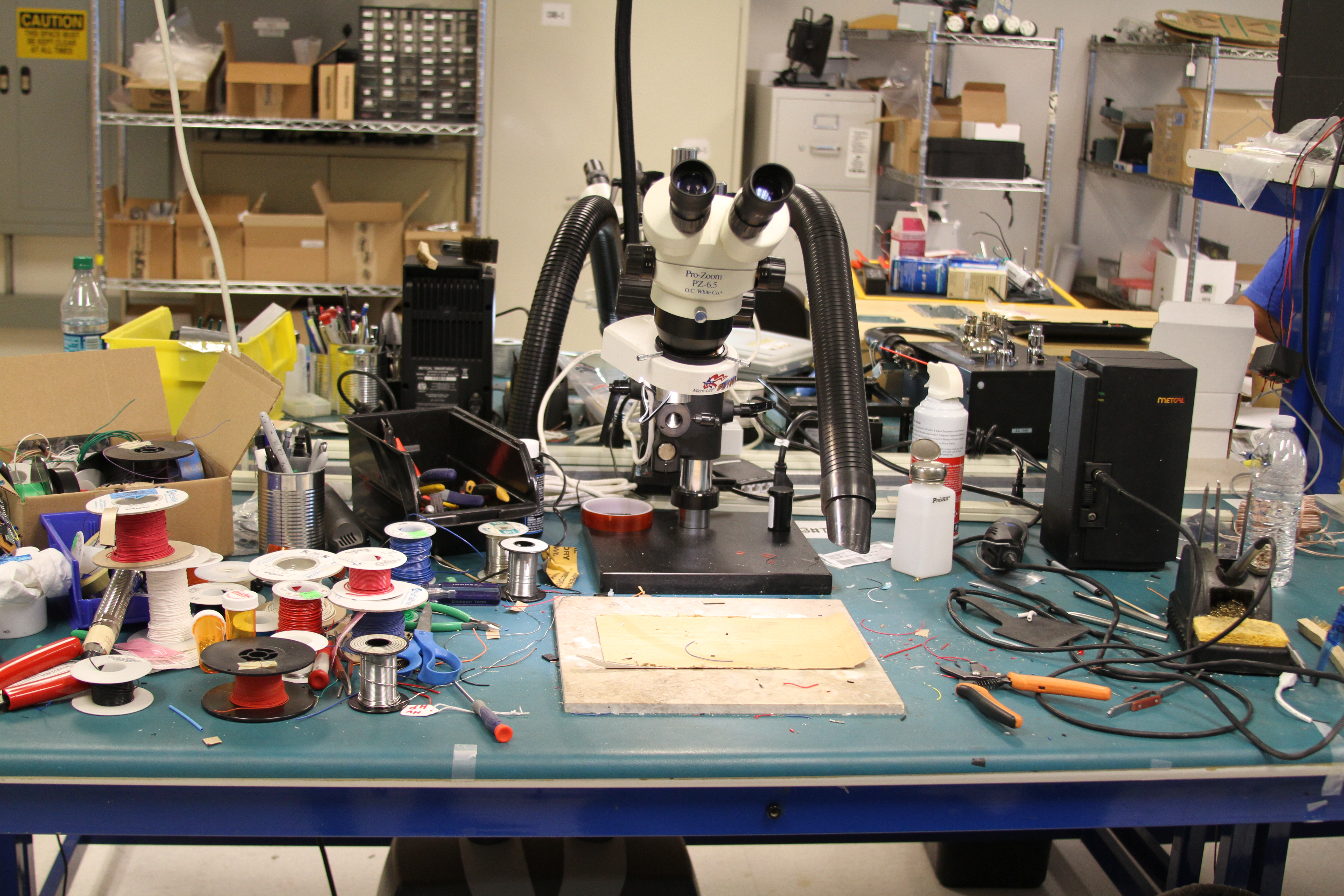
After lunch, we got to tour of a couple of labs. This workbench was well stocked with a Metcal soldering iron (our favorite) and lots of tools and supplies.
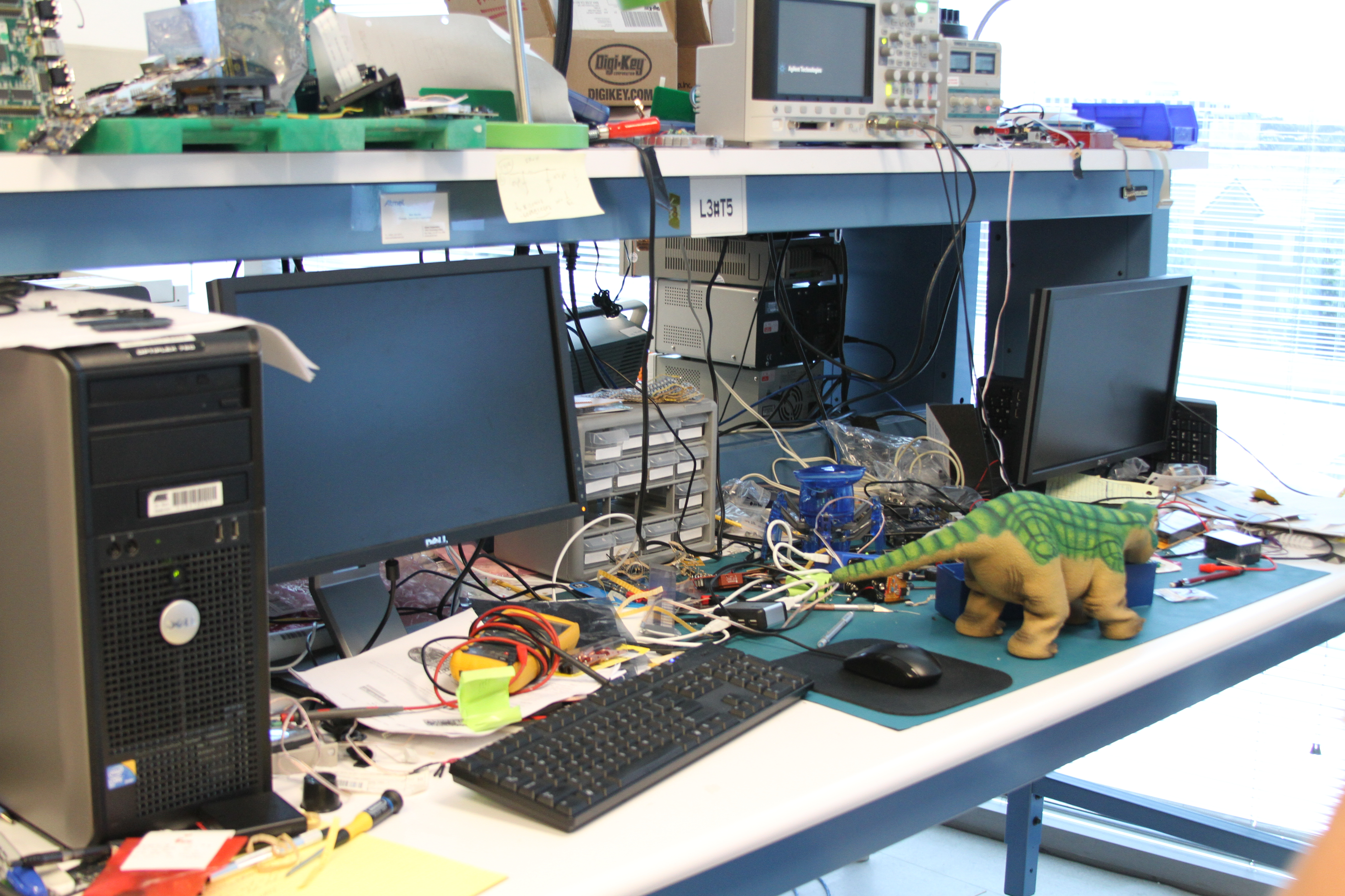
Apparently the poor Pleo on this bench needed some repair.
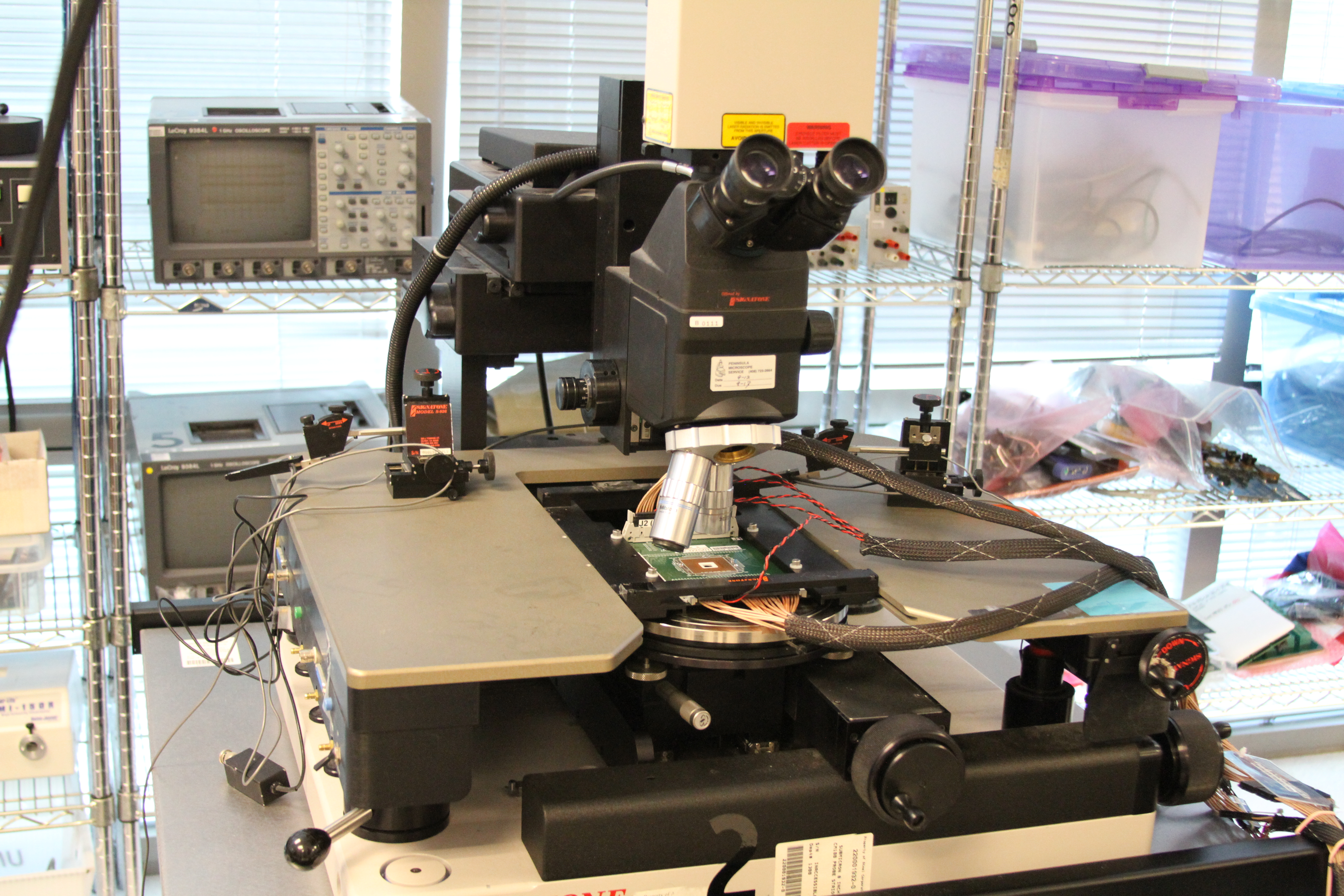
This machine is for inspecting and testing chips after they have been removed from their housing.
We got to go into the RF anechoic chamber, and watch as our cell phones stopped receiving any signals.
We also had some time to hang out and horse around with friends new and old. Our friend Paul Rako seemed to be having as much fun as the kids.
Photo courtesy of Atmel
Thanks to Paul and Atmel for inviting us to visit!
We found this gem in A Manual of Engineering Drawing for Students and Draftsmen, 9th Ed., by French & Vierck,1960, p. 487.
Printed Circuits allow miniaturization and the elimination of circuit errors—advantages that cannot be obtained by other methods. Once a pattern or suitable design is established, preparation of a black and white drawing can start. Scales for reduction, for example, 4 to 1, 3 to 1, or 2 to 1, are used. To insure sufficient bonding area of the metal laminate during soldering operations, lines should not be less than 1/32 inch in width when reduced. Line separation should never be closer than 1/32 inch on the final circuit. Figure 19.24 illustrates the drawing of printed circuits.
Peter wrote in about his experience with the Digi-Comp II:
I just wanted you and the entire Evil Mad Scientist team to know that the Digi-Comp II was a big success. I used it to explain digital computers to a group of second graders and fifth graders. In an age of iPads and smartphones, it’s surprisingly hard to demonstrate the beauty and magic of digital computer. The Digi-Comp II was perfect, looked great, and worked flawlessly. Thanks!
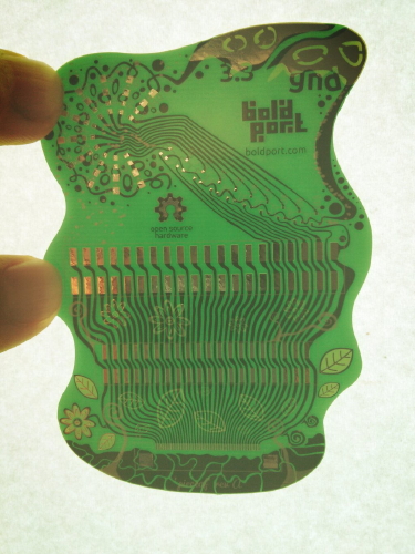
The folks at BoldPort have created PCBmodE, free open source software for designing printed circuit boards, but with an artistic perspective. Traditional EDA tools are designed from an engineering perspective, whereas PCBmodE treats the PCB as a creative palette. They aim to give you freedom to express your design with all the tools of the medium.
We wanted to create circuit boards that have curvey traces, meandering paths, and multiple soldermask layers, so we developed PCBmodE (say “PCB mode”), an open source Python software that unshackle us from the constraints imposed by traditional PCB design tools. We use the power of Inkscape — the leading open source vector graphics editor — to achieve any shape imaginable. Together with our powerful back-end tools, we can manufacturable beautifully functional boards.
They’ve posted about several of their example boards including pieceof (pictured above), a Raspberry Pi daughterboard called shimmy, and a tribute board dedicated to Bob Pease. This is a really neat approach to building circuit boards, and it looks like it has a lot of potential.
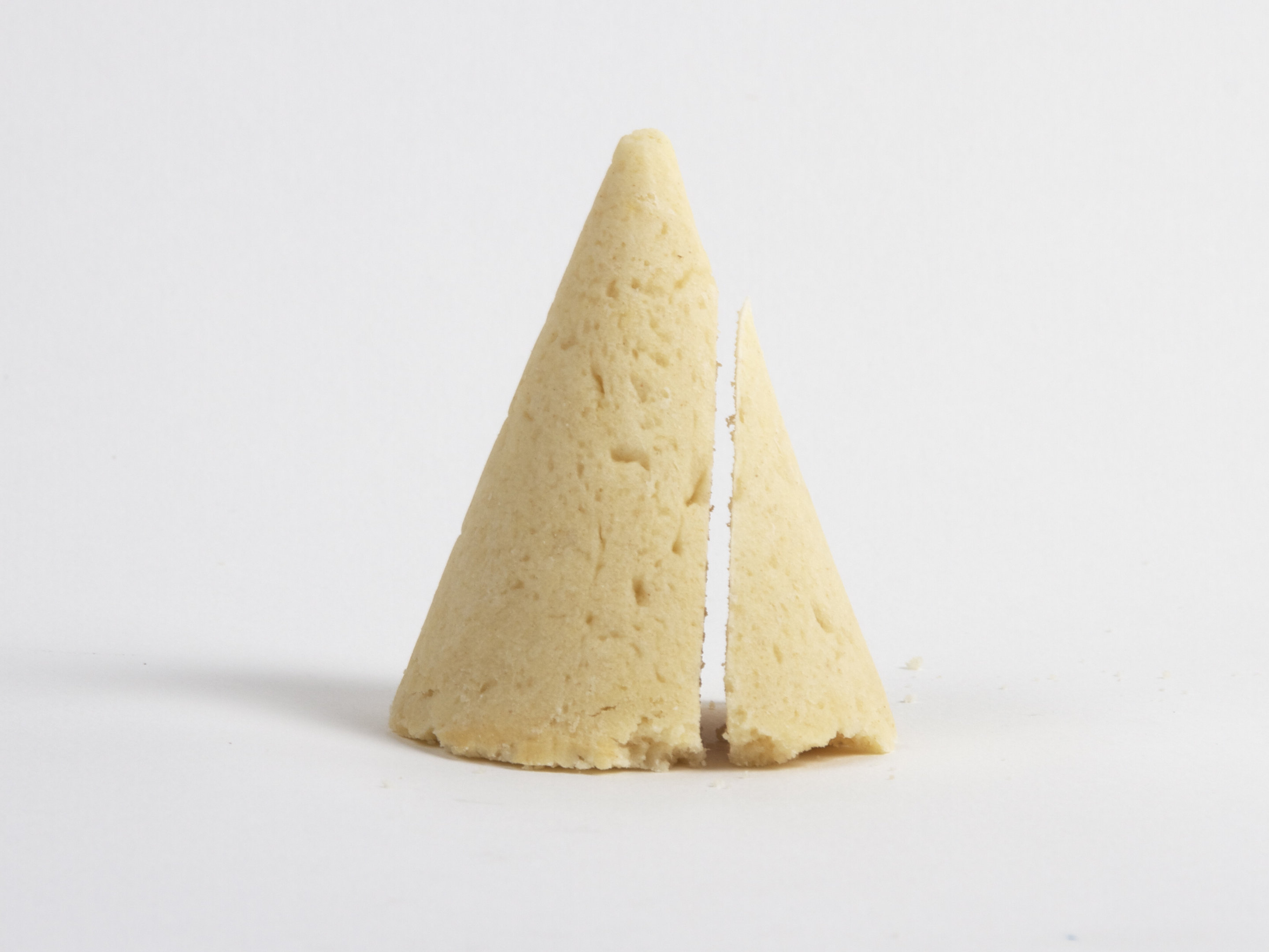
The scone is a classic single-serving quick bread that is often served with breakfast or tea.
And, at the intersection of the two, we present something entirely new, delightfully educational, and remarkably tasty: Sconic Sections.
In what follows, we’ll show you how to bake cone-shaped scones, to slice them into plane geometric curves, and to highlight those curves by selective application of toppings. We’ll also discuss some of the methods that didn’t work so well, as we refined our methods for making these.
Onwards, towards parabolic preserves and hyperbolic Nutella!
You may already be familiar with Super Awesome Sylvia, who has been working hard with us on the WaterColorBot toward our planned launch in July. Sylvia was just featured in the June 24 issue of People Magazine. Way to go, Sylvia!
The self anchored suspension span tower comes into focus, after crews dismantled the scaffolding that supported the 525-foot tower. Courtesy of Caltrans.
Here in the San Francisco Bay area, we’ve been watching the progress of the replacement of the east span of the Bay Bridge, which connects San Francisco to Oakland via Yerba Buena Island.
A look inside the East Span’s Splay Saddle, where the main cable wraps around the west end of the bridge. Courtesy of Caltrans
The California Department of Transportation has been doing an incredible job of sharing the progress with the public since construction began in 2002. The latest set of drool-worthy engineering photos is up on the Bay Bridge Info site, giving a peek deep inside the project.
Sparks fly as workers cut into the shear keys at Pier E2. Bay Bridge crews have been hard at work repairing broken rods on the eastern span. Courtesy of Caltrans
The media archive chronicles the project since its start in video and pictures, so you can delve even deeper. You can also follow @BayBridgeInfo on twitter for updates. The new bridge is nearing completion, and is scheduled to open Labor Day weekend this year.
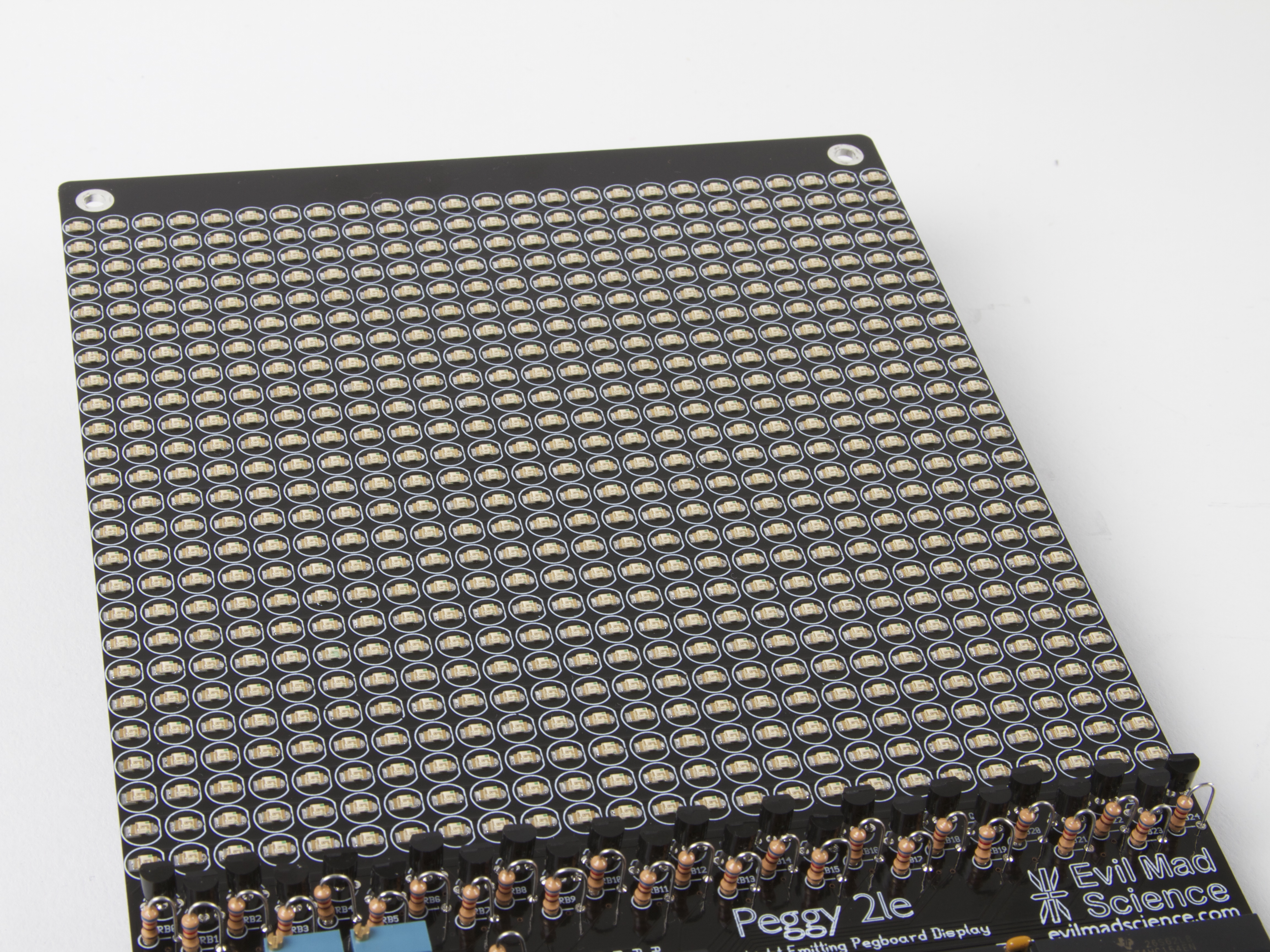
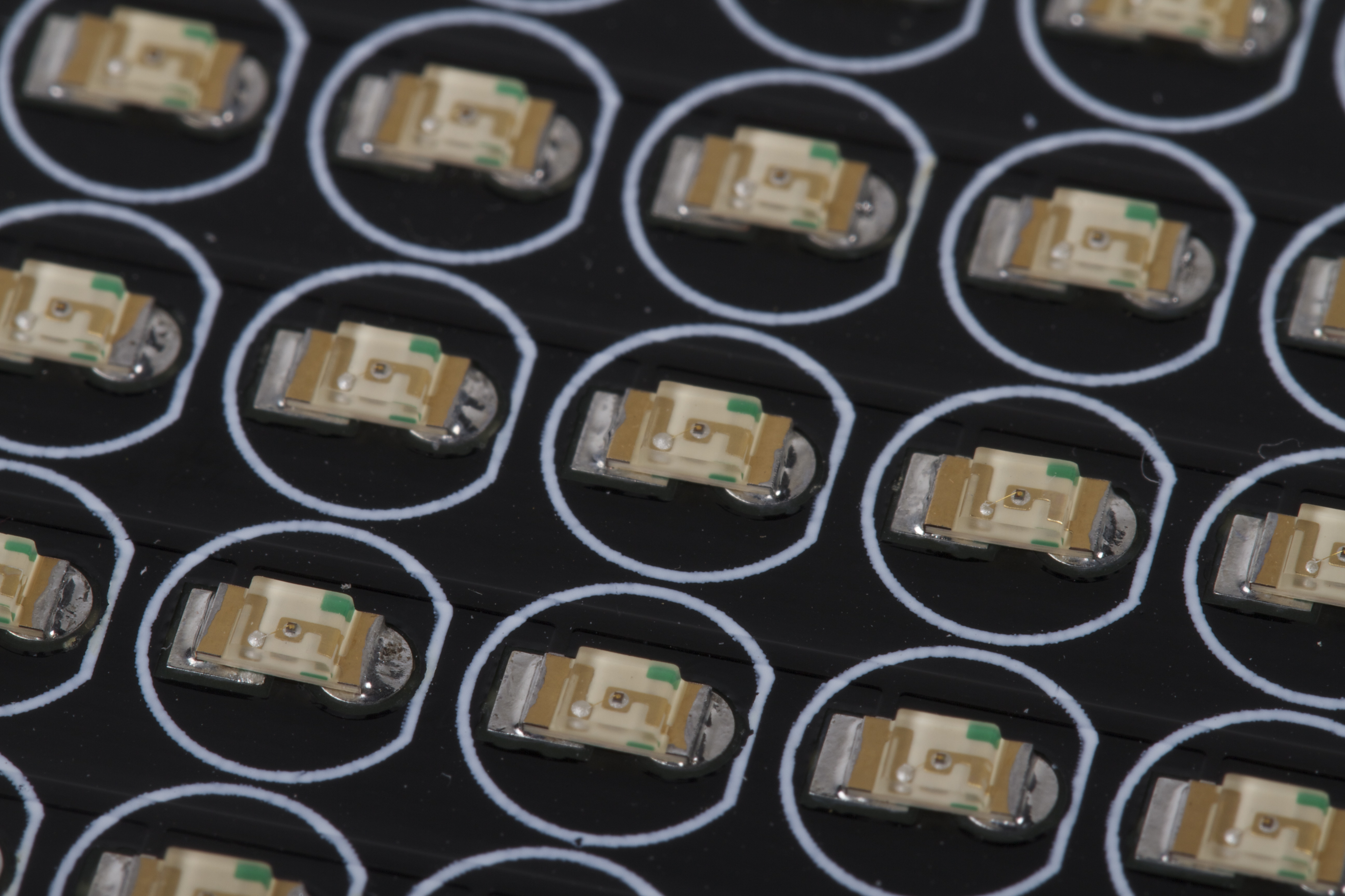
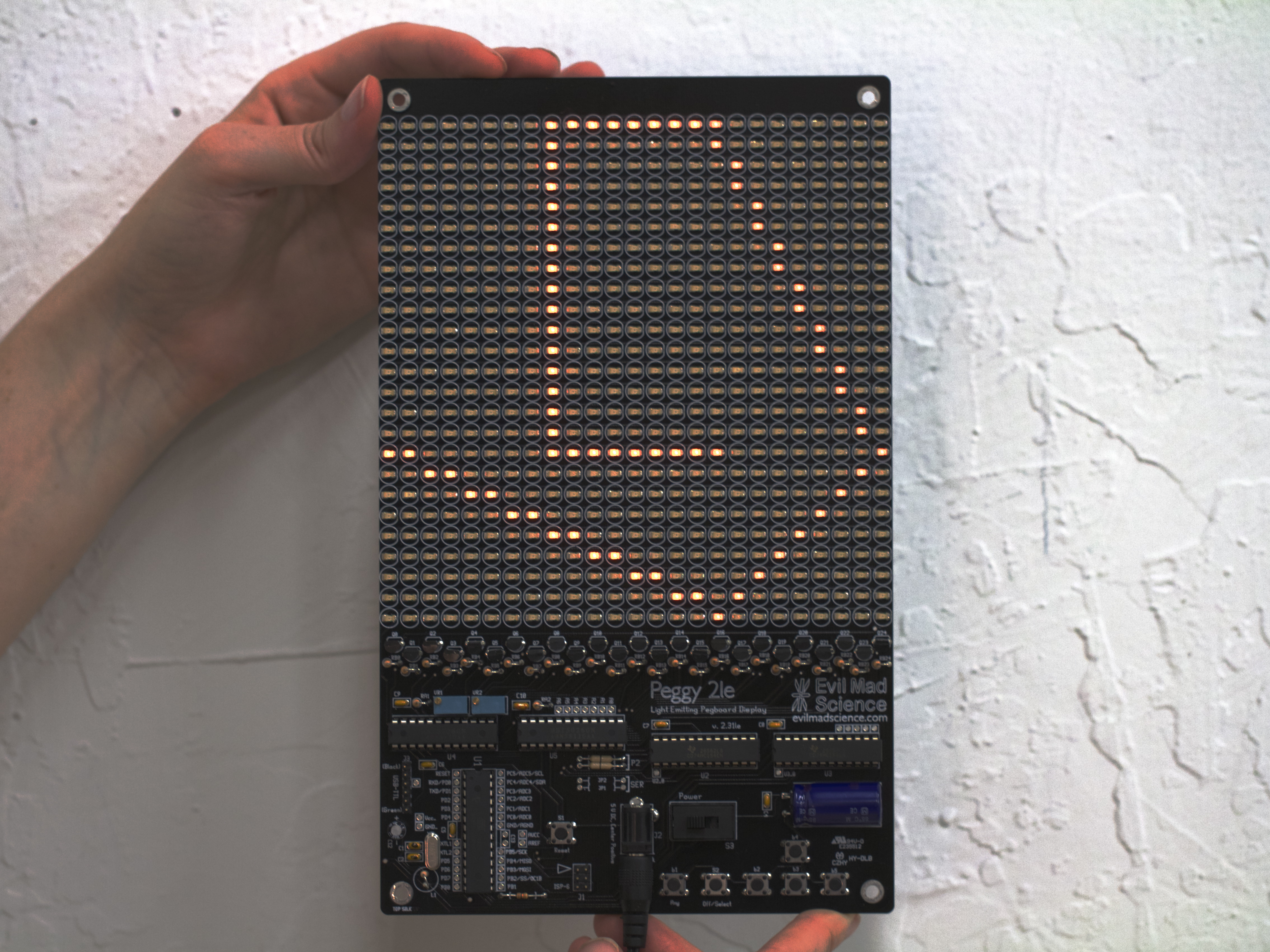
Peter T. recently stopped by our shop with his Peggy 2LE and showed us his incredibly cool hack. He had noticed that the 0.1″ pin spacing for a standard through-hole LED is just about perfect to accommodate LEDs in a 1206 surface mount package.
Once he had finished populating all the LED locations, he brought it by again. He used an alignment jig he had made to keep everything in straight rows while soldering.
The surface mount LEDs look great on the grid designed for T-1 3/4!
We plugged it in so we could see his pretty orange LEDs in action. Thanks to Peter for bringing it by and letting us take pictures!