Home › Evil Mad Scientist Forums › Ask an Evil Mad Scientist › Layers of a pcb
- This topic has 3 replies, 2 voices, and was last updated 12 years, 7 months ago by Windell Oskay.
Viewing 4 posts - 1 through 4 (of 4 total)
-
AuthorPosts
-
September 4, 2012 at 4:04 pm #20112RobotGrrlParticipant
Hi there,
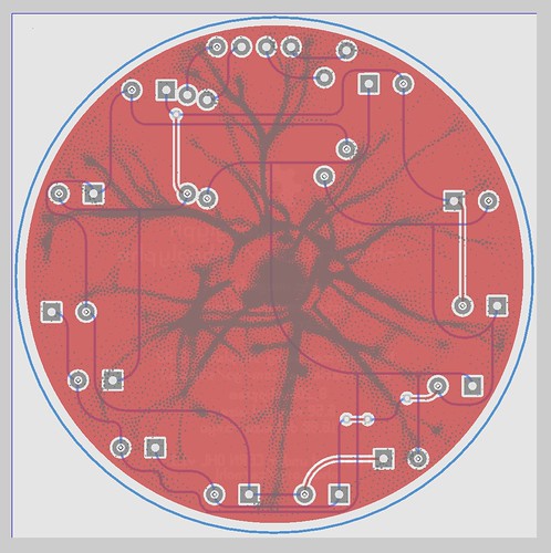
I’m trying to make a board that has some art on the ‘shiny’ layer (the ‘pins and pads’) layer in geda. The artwork appeared to be okay, and the soldermask layer was not covering it.Here’s what it looked like in geda: Here’s a pic of the soldermask layer on: http://www.flickr.com/photos/robotgrrl/7687135018/in/set-72157630843963020/When I was having the boards made, the manufacturer said to put a fill on the top layer, otherwise it would be the pcb material that would show through. However, when I received the boards, there was no artwork showing. :|Here’s a picture of the gerber, this is the top layer. From left to right is: first version without fill, second version with fill, third version with cleaned up fill.
 And after the top layer, this is what is below:
 Questions:Why did it turn out the way it did?What changes can be made to fix it (so the artwork would be shiny)?What layer should I put the artwork on (in geda)? What layer would this be in the gerber?Was the fill needed, or was that what caused it to mess up?Hopefully you can help point me in the right direction at least! If it helps, you can download and look at the board from here: https://github.com/RobotGrrl/PlasmaRoboGlyphThanks geda guru :)September 4, 2012 at 5:43 pm #20913Windell OskayKeymaster
Hi RobotGrrl,
I’m sorry to see that it didn’t turn out– it looked pretty good a few weeks ago in gEDA. :(From a quick glance at your Gerbers, I would have guessed that your top side would have had a nearly-solid copper layer across the top, and that you would have had soldermask holes through it, showing the “plasma” pattern in exposed copper (likely either gold or solder plated copper). I do think that I see what what might have gone wrong, however.It seems as though your “plasma” pattern is not made up of little circles, but of *really* little square pixels, where each of those square pixels is only a few mils across– likely smaller than the minimum feature size of the soldermask from your PCB manufacturer. While the manufacturer may not be able to fabricate it as you drew it, they should have caught the error and asked you to revise it. So, this is at least partly a mistake on the fault of the manufacturer.In testing here, I was able to convert the SVG to a PDF, and then to use pstoedit to convert that to a PCB file, all while keeping the original circle shapes from the SVG file. That can then be converted into a footprint, to clear the soldermask from the PCB. Alternately, you can create a second “copper” layer that contains the original pattern, and then manually merge the gerber for that layer with the gerber for the soldermask, to create extra holes in your soldermask, even without doing it directly in PCB.What route did you use, such that you ended up with the pixelation?September 4, 2012 at 7:06 pm #20914RobotGrrlParticipantSo what actually exposes the copper are holes in the soldermask? Or both the holes in the soldermask and holes in the fill?
I’ll try to make the fill have holes in the shape of the pattern.The route that I used was from Inkscape to a .png image, then to a Processing sketch I wrote to make tiny squares that would be on the pins and pads layer. Thought everything on that layer would then be exposed copper.September 4, 2012 at 8:15 pm #20915Windell OskayKeymasterIf you look at the gerber of a soldermask layer, what you’ll find is that it’s actually a negative layer. Soldermask goes everywhere on your PCB except where you have features in that gerber layer. And yes, you need to have holes in the soldermask around every pin and pad that you want electrical connections to, because you can’t make electrical connections through the soldermask.
By default, gEDA puts a hole in the soldermask around every SMT pad in a footprint, which is how it generated the holes in the soldermask above your footprint.For the next round, you should probably skip the .png portion; you could even modify StippleGen to output your pins and pads, so that you skip inkscape entirely. :)Also, it’s a *very* good idea to run the DRC (design rule check) on your PCB before even exporting to gerber. It will make sure that you don’t have any features (let alone 20,000) that are too small to fabricate. -
AuthorPosts
Viewing 4 posts - 1 through 4 (of 4 total)
- You must be logged in to reply to this topic.


